In the world of electronics manufacturing and repair, precision is everything PCB Microscopes . As printed circuit boards (PCBs) have become smaller and more complex, the need for accurate inspection tools has grown exponentially. Among the most crucial tools used by engineers, technicians, and electronics hobbyists is the PCB microscope.
This article explores what PCB microscopes are, their types, features, applications, and how to choose the best one for your needs.
What is a PCB Microscope?
A PCB microscope is a specialized optical instrument used for inspecting and analyzing printed circuit boards. Unlike general-purpose microscopes, PCB microscopes are tailored to electronics work—allowing users to examine small components, fine solder joints, and microscopic traces on the board. These microscopes help identify defects such as cold solder joints, solder bridges, and component misalignment, and are essential for tasks like soldering and desoldering surface-mounted devices (SMDs).
Why Are Microscopes Essential for PCB Work?
Modern PCBs feature tiny components, including microchips and resistors that are barely visible to the naked eye. With surface mount technology (SMT) dominating the industry, components are densely packed, increasing the likelihood of manufacturing or assembly defects.
Here’s why microscopes are vital in PCB inspection:
- Enhanced visibility of fine details
- Increased accuracy during rework or component placement
- Defect detection before product failure
- Quality assurance in manufacturing processes
Types of PCB Microscopes
PCB microscopes come in various types depending on their features, optics, and intended use. The main types include:
1. Stereo Microscopes
Also known as dissecting microscopes, these provide a three-dimensional view of the PCB. They are ideal for soldering tasks and visual inspection.
Pros:
- Great depth perception
- Wide field of view
- Easy to use with tweezers or soldering irons
Cons:
- Limited magnification (typically up to 50x)
- Not suitable for extremely small components like micro BGAs
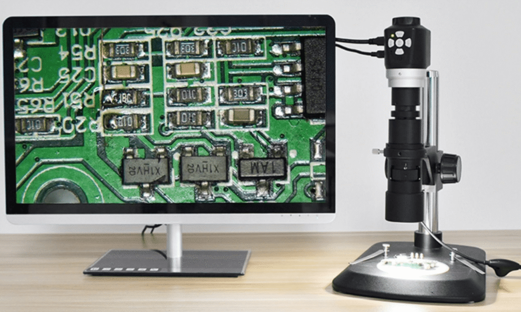
2. Digital Microscopes
These are modern microscopes with built-in digital cameras that display the magnified image on a monitor. They often include features like image capture, measurement tools, and HDMI output.
Pros:
- Ergonomic (view on screen, not through eyepieces)
- Recordable video and images
- High magnification levels (up to 1000x)
Cons:
- Some low-end models may have lag or poor image quality
- Depth perception may be limited
3. USB Microscopes
Compact and affordable, USB microscopes connect directly to a computer via USB. They are ideal for beginners or casual inspection work.
Pros:
- Inexpensive and portable
- Easy setup
Cons:
- Limited durability
- Lower image quality
- Not ideal for continuous professional use
4. Metallurgical Microscopes
These high-end microscopes are used for in-depth analysis and failure diagnostics, often in research and development or forensic electronics.
Pros:
- High precision and magnification
- Excellent for internal layer inspection
Cons:
- Expensive
- Overkill for general electronics repair
Key Features to Look for in a PCB Microscope
When choosing a microscope for PCB inspection, consider the following essential features:
1. Magnification Power
A good range is 10x to 100x for most electronics tasks. SMD components typically require 20x–70x magnification for detailed viewing.
2. Working Distance
This is the distance between the objective lens and the work surface. A longer working distance allows more space for tools and components.
3. Illumination
Proper lighting is critical. Many microscopes include LED ring lights, adjustable brightness, and diffusers to eliminate glare.
4. Ergonomics
For professionals working long hours, microscope ergonomics matter. Adjustable stands, screen displays, and headrest eyepieces reduce fatigue.
5. Camera Integration
Digital and USB microscopes often come with image capture and measurement software, beneficial for documentation or training.
6. Stability and Build Quality
Look for a solid, vibration-free stand and base to maintain image clarity during detailed work.
Common Applications of PCB Microscopes
PCB microscopes serve various industries and purposes, including:
• Soldering and Rework
SMD soldering under a microscope improves precision, especially with micro-components like 0402 resistors or QFN packages.
• Inspection and Quality Control
Manufacturers use microscopes to inspect every board for defects before shipment.
• Failure Analysis
When a PCB fails, microscopes help identify broken traces, burnt components, or soldering errors.
• Educational and Training Labs
Used in teaching environments to demonstrate micro-electronics and assembly techniques.
• Reverse Engineering
Helpful when studying legacy boards or creating schematics from undocumented PCBs.
Maintenance Tips for PCB Microscopes
To ensure longevity and consistent performance, follow these maintenance practices:
- Keep lenses clean using a microfiber cloth and lens cleaning solution.
- Avoid harsh chemicals near optical components.
- Cover the microscope when not in use to prevent dust buildup.
- Check light sources regularly and replace burned-out LEDs.
- Secure cables and connections to avoid strain or damage.
Future Trends in PCB Microscopy
As PCBs continue to shrink and become more complex, microscope technology is also evolving. Some upcoming innovations include:
- AI-assisted defect detection
- 3D imaging and holographic visualization
- Wireless digital microscopes
- Integration with AR/VR for enhanced inspection
These advancements promise to make inspections more accurate, efficient, and accessible, especially in high-volume production environments.
Conclusion
PCB microscopes are indispensable tools in modern electronics design, repair, and manufacturing. Whether you’re a seasoned engineer or an electronics enthusiast, the right microscope enhances your ability to work with tiny components, ensures quality, and reduces costly errors.
By understanding the types, features, and applications of PCB microscopes, you can confidently invest in the right equipment for your workbench or production line. Precision matters—and with a microscope, you’ll see the difference clearly.
FAQs
Q1: What magnification is best for PCB inspection?
A: 10x to 70x is ideal for most PCB tasks. For micro-components, 40x to 100x may be necessary.
Q2: Can I solder while using a microscope?
A: Yes. Stereo and digital microscopes with long working distances are perfect for soldering and rework.
Q3: Are USB microscopes good for PCB repair?
A: They are suitable for basic tasks or hobby use, but may lack the precision and image quality required for professional work.
Q4: What is the difference between a stereo and digital microscope?
A: A stereo microscope offers 3D viewing through eyepieces. A digital microscope displays the image on a screen, often with additional features like recording and measurement.
Q5: Do PCB microscopes require calibration?
A: Most optical microscopes do not require frequent calibration, but digital ones may need software updates and alignment checks.